
The global chip demand continues to skyrocket with no signs of slowing down. The Semiconductor Industry Association is reporting first-quarter sales hitting an incredible $298.5 billion. So, the pressure on manufacturing facilities is immense. Moving highly advanced chip designs from a digital blueprint into high-volume physical production has become one of the most complex computational challenges in modern tech history. To tackle this hurdle head-on, TSMC is bringing NVIDIA chip manufacturing AI frameworks straight onto the factory floor. This way, they’re optimizing every stage of the silicon lifecycle.
Accelerating physics and computational chemistry
Under this partnership, TSMC is using CUDA-X libraries to boost intense physical simulations. For instance, TSMC deployed a GPU-accelerated library called cuLitho to handle computational lithography. This one manages the complex printing process for chip mask designs. This software shift brings a 20% to 50% improvement in cost-effectiveness and cycle times compared to older CPU-based setups.
The optimization extends down to basic material chemistry. There’s also the cuEST electronic structure simulation library. cuEST enables TSMC engineers to run chemistry simulations for material design an average of 50 times faster. To keep the physical factories running at maximum efficiency, TSMC uses NVIDIA H200 GPUs to compute complex scheduling constraints. This accelerates production paths and maximizes daily output.
Catching nanometer defects and building digital twins
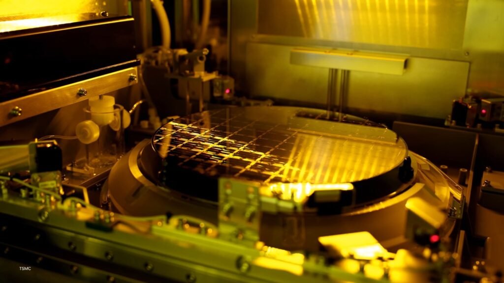
With individual advanced silicon wafers costing up to $20,000, even a minor mistake can cause millions in losses. To combat this, TSMC is integrating the NVIDIA Metropolis platform and the TAO Toolkit into its visual inspection systems. With vision AI, the foundry has massively enhanced its ability to classify and catch nanometer-scale defects. It also successfully reduces the time-consuming need for engineers to repeatedly label data and retrain models.
Furthermore, TSMC is planning for future expansions by exploring Omniverse libraries to construct a virtual factory environment called FabTwin. This digital twin allows management to evaluate machine layouts and test complex manufacturing scenarios virtually before committing any real-world capital.
A quiet expansion into healthcare
The manufacturing updates showcase how deep NVIDIA’s roots go inside the silicon supply chain. However, the company separately also revealed that its software ecosystem is expanding into clinical spaces. Partnering with Foxconn, the technology stack is moving across medical centers in Taiwan. Foxconn is migrating from fragmented digital tools to fully coordinated AI agent workforces. Their CoDoctor AI platform and the Nurabot nursing collaborative robots—now powered by the secure NemoClaw architecture—have officially transitioned out of experimental pilot phase. Now it’s in active clinical operations to assist healthcare workers with real-time documentation and patient care coordination.
The post TSMC Is Using NVIDIA AI to Build the Next Generation of Silicon appeared first on Android Headlines.